(Nanowerk News) Progress in the field of linked tours is measured by matching, exceeding, or falling behind the level set by Gordon Moore, former Chief Executive and co-founder of Intel, which said the number of electronic components, or transistors, per integrated circuit would double each year. That was over 50 years ago, and surprisingly his prediction, now known as Moore’s Law, came true.
In the last few years, the pace was thought to have slowed; one of the biggest challenges in putting more cycles and power on a smaller chip is heat regulation.
A multidisciplinary group comprising Patrick E. Hopkins, a professor in the Department of Mechanical and Aerospace Engineering at the University of Virginia, and Will Dichtel, a professor in the Department of Chemistry at Northwestern University, is designing a class new material with the ability to hold chips. cool how to keep shrinking in size – and to help Moore ‘s Law come true.
Their work was recently published in Nature’s products (“Ultra-low-k thermal conductivity dielectric arrays based on covalent two-dimensional organic frames”).
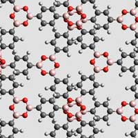
Electrically insulating materials that reduce electrical crosstalk in dielectrics are called “low-k”. This type of material is the silent hero that makes all electronics possible by directing the current to eliminate erosion and signal interference; if possible, it can also attract destructive heat by an electric current away from the circuit. The heat problem becomes exponential as the chip becomes smaller because not only are there more transistors in a particular area, which produces more heat in that same area, they are closer on each other, which makes it harder to dissipate heat.
“Scientists have been finding a low-k dielectric material that can handle heat transfer and space issues inherent in much smaller blades,” Hopkins said. “While we have come a long way, new developments are not going to happen unless we put together topics. For this project we have applied research and principles from a number of fields – mechanical engineering, chemistry, materials science, electrical engineering – to solve a difficult problem that none of us could work out on our own. ”
Hopkins is one of the leaders of UVA Engineering’s Multifunctional Material Integration campaign, which brings together researchers from multidisciplinary engineering to create products with a wide range of responsibilities.
“Seeing my ‘problem’ through someone else’s lens in a different field was not only interesting, it inspired ideas that eventually led to progress. I think it got we all have that experience, “said Ashutosh Giri, a former UVA Engineering and Ph.D. D. a student at the Hopkins Laboratory, co-author of a Natural Materials paper and assistant professor of mechanical, industrial and systems engineering at the University of Rhode Island.
“The heart of the project was when the chemical team understood the thermal activity of their material, understood a new dimension about their work, and when the mechanical and materials team understood the level of molecular engineering that chemistry was capable of,” said Giri.
“We take sheets of polymer that are only one thick atom – this is what we call 2D – and control their properties by placing the sheets in a special architecture,” said Dichtel .
“Our efforts on the development of the techniques to make high-quality 2D polymer films have allowed this collaborative work.”
The team is applying this new product class to try to meet the requirements of miniaturizing transistors on a dense chip, Dichtel said.
“This has great potential for use in the semiconductor industry, the chip manufacturing industry. It has both low electrical conductivity, or ‘low-k,’ and high heat transfer capacity,” he said. .
This combination of buildings has recently been identified by the International Roadmap for Semiconductors as a prerequisite for next generation integrated circuits.
“For this project, we are focusing on the thermal properties of this new material class, which is wonderful, but even more interesting is that we are just scratching the surface,” said Austin Evans, Ph.D. A student at Northwestern ‘s Dichtel Lab and first co – author of Nature Materials. “Developing new classes of materials with a unique mix of properties has incredible technological potential.
“We are already studying this new class of materials for many applications, for example, chemical sensing. We can use these materials to find out – ‘sensitivity’ – what chemicals are and the level of these chemicals in the air.This has a wide range of effects.For example, by knowing the chemicals in the air, we can increase food storage, transport and circulation to global food waste As we continue to explore, we are likely to find more features that are unique to these new products, “Evans said.