, which combines images with spectroscopy, to observe metallic properties in the perovskite crystal barium stannate (BaSnO3). The resolution-atomic STEM image, with a BaSnO3 crystal structure (left), shows an irregular arrangement of atoms identified as the heart of a metallic line defect. Credit: Mkhoyan Group, University of Minnesota")
Professor K. Andre Mkhoyan from the University of Minnesota and his team used scanning electron diffusion electron microscope (STEM), which combines images with spectroscopy, to observe metallic properties in the perovskite crystal barium stannate (BaSnO3). The resolution-atomic STEM image, with a BaSnO3 crystal structure (left), shows an irregular arrangement of atoms identified as the heart of a metallic line defect. Credit: Mkhoyan Group, University of Minnesota
In advanced materials research, a team led by Professor K. Andre Mkhoyan of the University of Minnesota has found that combines the best of two features sought after for touch screens and smart windows – transparency and cunning.
The researchers were the first to observe metallic lines in perovskite crystals. Perovskites are abundant in the center of the Earth, and barium stannate (BaSnO3) is one such crystal. However, metallic buildings have not been extensively studied due to the prevalence of more conductive materials on the planet such as metals or semiconductors. The discovery was made using an advanced electronic transmission microscope (TEM), a method that can produce images with magnifications of up to 10 million.
The research is published in Advances in science.
“The favorable behavioral and directional nature of these metallic line defects means that we can produce a material that is visibly glassy and at the same time very subtle as a metal,” said Mkhoyan, a TEM expert and Ray D. and Mary T. Johnson / Mayon Plastics Chair in the Department of Chemical and Materials Science at the University of Minnesota College of Science and Engineering. ”This will give us the two best of both worlds. We can make windows or new types of touch screens visible and at the same time directional. This is very interesting. “
Defects, or imperfections, are common in crystals – and line defects (the most common of which are separations) are a series of atoms that change from the normal order. Since dislocations have the same combination of elements as the host crystal, the changes in electronic band structure are usually not at the heart of dislocation, due to reduced symmetry and strain, but slightly different than the. the guest. The researchers had to look outside the disorders to find the metallic line defect, where the shape of a defect and the resulting atomic structure are quite different.
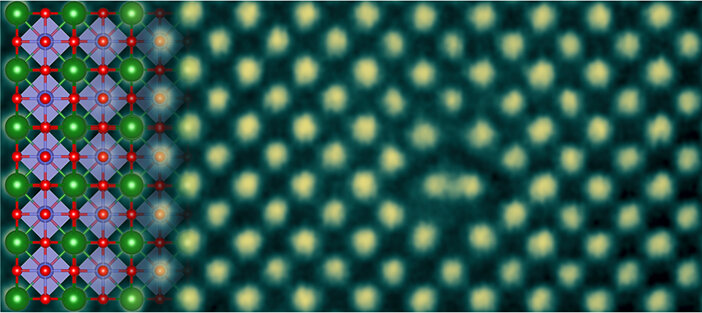
 at a 10 million-fold magnitude, University of Minnesota researchers were able to separate the structure and composition of the metallic line defect and image in a BaSnO3 perovskite crystal. This image shows the atomic arrangement of both the BaSnO3 crystal (left) and the defect of the metabolic line. Credit: Mkhoyan Group, University of Minnesota")
Using an advanced scanning diffusion electron scanning electron microscope (STEM) at a 10 million-fold magnitude, University of Minnesota researchers were able to separate the structure and composition of the metallic line defect and image in a BaSnO3 perovskite crystal. This image shows the atomic arrangement of both the BaSnO3 crystal (left) and the defect of the metabolic line. Credit: Mkhoyan Group, University of Minnesota
“We have easily seen these line defects in the high-scan diffusion electron microscopy images of these BaSnOs.3 thin films because of their unique atomic arrangement and we only saw them in the vision of the plan, “said Hwanhui Yun, a graduate student in the Department of Chemical Engineering and Materials Science and lead author of the study.
For this study, BaSnO3 films were grown with molecular beam epitaxy (MBE) – a method for making high-quality crystals – in a laboratory at the University of Minnesota’s Twin Cities. Metal line problems observed in these BaSnOs3 films move forward in the direction of film growth management, which means that researchers can control how or where line defects appear – and can innovate as needed. the touch screens, smart windows and other future technologies that require a combination of brightness and conductivity.
“We need to be creative to grow high quality BaSnO3 thin films using MBE. It was inspiring when these new line defects came to light in the microscope, ”said Bharat Jalan, an associate professor and Chair of Shell in the Department of Chemical Engineering and Materials Science, which oversees the work- blade forming a mixture of perovskite oxide films with MBE.
Perovskite crystals (ABX3) there are three elements in the unit cell. This gives it freedom for structural changes such as crystal composition and symmetry, and the ability to accommodate a number of defects. Due to different co-ordination and connection angles of the atoms in the core of the line fault, new electronic states are introduced and the structure of the electron band is changed locally in such a remarkable way that it turns the line fault into metal.
“It was interesting how theory and experiment agreed together here,” said Turan Birol, an assistant professor in the Department of Chemical Engineering and Materials Science and an expert in density action theory (DFT). “We were able to validate the experimental observations on the atomic structure and electron properties of this line with the main principles of DFT computation.”
To read the full research paper titled “Metal line cracking in BaSnO3 wide bandwid perovskite,” visit Advances in science website.
Scientists measure local cracking methods at individual crystalline cracks
Hwanhui Yun et al, Metallic line cracking in BaSnO perovskite wide-bandgap.3, Advances in science (2021). DOI: 10.1126 / sciadv.abd4449
Presented by the University of Minnesota
Citation: The behavioral nature of crystal structures published at 10 million times size (2021, January 15) was retrieved January 16, 2021 from https://phys.org/news/2021-01-nature-crystal-revealed-magnification -million.html
This document is subject to copyright. Other than any fair treatment for the purpose of scrutiny or private investigation, no part may be reproduced without written permission. The content is provided for informational purposes only.